Scroll to:
Structure and properties of two-layer coatings in the HfSi2–HfB2–MoSi2 system produced by electrospark deposition and magnetron sputtering
https://doi.org/10.17073/1997-308X-2025-3-48-59
Abstract
A two-layer coating with a total thickness of approximately 15 μm was obtained using a combined technology of electrospark deposition (ESD) and high-power impulse magnetron sputtering (HiPIMS), employing HfSi2–HfB2–MoSi2 ceramic electrodes/target on a niobium substrate. The formation mechanism, morphology, and structure of the coatings were investigated using glow discharge optical emission spectroscopy (GDOES), scanning electron microscopy (SEM), and transmission electron microscopy (TEM). It was found that the ESD coating consists of 65 wt. % phases formed through interaction between the electrode and the substrate – namely NbSi2 and Nb5Si3 – and exhibits a silicon concentration gradient (from 8 to 54 at. %) across the coating thickness, from the substrate toward the surface. The outer amorphous HiPIMS coating is ~5 μm thick. Analysis of structural and phase transformations during heating of the ESD coatings up to 900 °C showed that annealing leads to its separation into two layers: an inner layer composed of dendritic grains of the metastable γ-Nb5Si3 phase and an outer layer based on NbSi2 . The HiPIMS coating crystallizes sequentially, forming (Hf,Mo)B2 at 700 °C, MoSi2 at 800 °C, and Hf3Si2 and HfSi2 at 900 °C, with the silicon content remaining virtually unchanged. As a result of the two-stage deposition process and subsequent high-temperature annealing, a multilayer protective ceramic coating was obtained, consisting of an outer layer of (Hf,Mo)B2–MoSi2–HfSi2 , an intermediate layer of NbSi2 , and an inner layer of Nb5Si3 , with hardness values of 9.4, 23.3, and 19.4 GPa, respectively. This coating significantly extends the service life of niobium grade Nb-1.
Keywords
For citations:
Zamulaeva E.I., Loginov P.A., Kiryukhantsev-Korneev P.V., Shvindina N.V., Petrzhik M.I., Levashov E.A. Structure and properties of two-layer coatings in the HfSi2–HfB2–MoSi2 system produced by electrospark deposition and magnetron sputtering. Powder Metallurgy аnd Functional Coatings (Izvestiya Vuzov. Poroshkovaya Metallurgiya i Funktsional'nye Pokrytiya). 2025;19(3):48-59. https://doi.org/10.17073/1997-308X-2025-3-48-59
Introduction
The potential for using niobium and its alloys in components operating at high temperatures and in aggressive gaseous environments largely depends on the application of protective coatings [1; 2]. Among the most promising are coatings based on silicides such as NbSi2 [3–5], MoSi2 [6–8], NbSi2–MoSi2 [9], and NbSi2–HfSi2 [10], due to the formation of a SiO2 film on their surface at elevated temperatures. A characteristic feature of such coatings is the formation of an intermediate diffusion layer of Nb5Si3 . Since the enthalpy of formation of Nb5Si3 (–516.8 kJ/mol) is lower than that of NbSi2 (–161 kJ/mol) [11; 12], the Nb5Si3 layer forms first during thermochemical treatment and is subsequently transformed into the NbSi2 phase [3–12]. The rate of mutual diffusion between the coating and the substrate – which leads to coating thinning and, consequently, a reduction in performance – can be reduced by introducing diffusion barriers [13–15], modifying the coatings with diffusion inhibitors [16; 17], or forming additional layers of mullite (3Al2O3·2SiO2) [17; 18] or borosilicate glass (B2O3·SiO2 ) [19; 20]. Multilayer coatings can also be produced by combining several technological approaches in a single process [21; 22] or by employing two-stage processes [2; 17].
In [23], the feasibility of using heterophase electrospark coatings based on MoSi2–MoB–HfB2 to improve the performance of the heat-resistant nickel superalloy EP741NP was demonstrated. Enhancement of the oxidation resistance of electrospark coatings through the application of an upper magnetron-sputtered layer has been demonstrated for steels [24] and nickel alloys [25].
The aim of this study is to fabricate two-layer ceramic coatings on Nb-1 niobium using a combination of electrospark deposition (ESD) and high-power impulse magnetron sputtering (HiPIMS), and to investigate the effect of vacuum annealing on their composition, structure, and properties.
Materials and methods
The consumable ceramic electrodes and targets were produced by self-propagating high-temperature synthesis (SHS) from elements (wt. %: 59 Hf, 28 Si, 11 Mo, 2 B), followed by hot pressing of the synthesized products [26]. Both the ESD electrodes and the HiPIMS targets had the following phase composition (wt. %): hafnium silicide (34 HfSi2 ), molybdenum silicide (17 MoSi2 ), hafnium boride (19 (Hf,Mo)B2 ), elemental silicon (21 Si), and hafnium oxide (9 HfO2 ) [27]. The ESD electrodes were fabricated as rectangular rods measuring 4×4×50 mm, while the HiPIMS targets were discs with a diameter of 120 mm and a thickness of 10 mm.
The coatings were deposited onto Nb-1 niobium plates measuring 10×10×3 mm. The ESD process was carried out in an argon atmosphere using the Alier-303 Metal unit (Russia–Moldova) under the following parameters: discharge current 120 A, pulse frequency 3200 Hz, and pulse duration 20 µs. HiPIMS deposition was performed using a UVN-2M system equipped with a magnetron and ion source. Target sputtering was performed using the TruPlasma 4002 system (Trumpf, Germany) at an average power of 1 kW, with a peak power of up to 50 kW, peak current of 50 A, pulse frequency of 1 kHz, and pulse duration of 50 µs. The two-layer ESD + HiPIMS coatings were obtained by sequential application of the ESD and HiPIMS processes.
The microstructure and elemental composition were examined using an S-3400N scanning electron microscope (Hitachi High-Technology Corporation, Japan) equipped with a NORAN X-ray System 7 energy-dispersive X-ray spectroscopy (EDS) unit (Thermo Scientific, USA). Metallographic cross-sections were prepared using a Rotopol-21 polishing system (Struers, Denmark). Elemental depth profiling of the coatings was carried out by glow discharge optical emission spectroscopy (GDOES) using a Profiler-2 instrument (Horiba Jobin Yvon, France). Phase composition was determined by X-ray diffraction (XRD) using a DRON-4 automated diffractometer (Burevestnik R&D Center, Russia) with CuKα radiation over a 2θ range of 10–120°. The obtained X-ray diffraction patterns were analyzed using the JCPDS database.
To analyze the structural and phase transformations occurring in the coatings during heating, high-resolution transmission electron microscopy (HRTEM) and electron diffraction were used. The studies were carried out in the column of a JEM 2100 microscope (JEOL, Japan) during isothermal holding at temperatures of 400, 500, 600, 700, 800, and 900 °C for 20–25 min. The heating rate was 100 °C/min. The elemental compositions of the as-deposited coatings and those cooled from 900 °C were analyzed by EDS using an X-Max80T detector (Oxford Instruments, UK). Lamellae were prepared using focused ion beam (FIB) milling in a Scios DualBeam scanning electron-ion microscope (FEI, USA). Annealing of the coatings was performed in a VSl-16-22-U vacuum furnace (VakETO, Russia) at 900 °C for 30 min under low vacuum.
The hardness (H) and Young’s modulus (E) of the coatings were determined by selective nanoindentation [28] using a NanoHardnessTester (CSM Instruments, Switzerland) with Indentation 3.0 software, in accordance with GOST R 8.748–2011 (ISO 14577).
Results and discussion
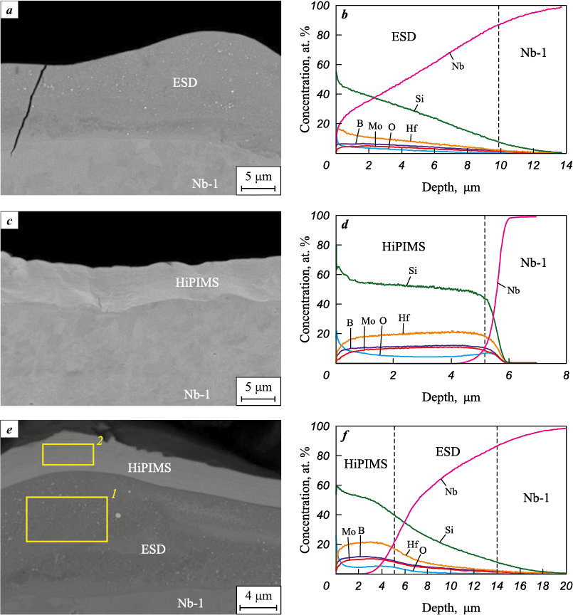
Despite the use of the same material as both the electrode and target for coating deposition, the layers formed by electrospark deposition (ESD) and high-power impulse magnetron sputtering (HiPIMS) differ in structure and phase composition. During ESD, due to high temperatures in the interelectrode gap, local melting of the electrode and the treated substrate occurs, resulting in a coating with a ~ 10÷12 thickness (Fig. 1, a). Across the coating thickness, from the surface toward the substrate, an elemental concentration gradient is observed: the niobium content increases from 18 to 85 at. %, while the contents of the electrode-derived elements Hf, Mo, B, O, and silicon decrease from 54 to 8 at. % (Fig. 1, b).
Fig. 1. Cross-sectional microstructures and GDOES profiles of coatings: (a, b); |
During HiPIMS, the coating is formed by atomic fluxes with a high fraction of ionized species and has a thickness of ~5 μm (Fig. 1, c). The elemental concentrations within the HiPIMS-deposited layer remain constant throughout its thickness, and no substrate material (Nb) is detected in the coating, which is confirmed by the sharp interface (Fig. 1, d).
In sequentially deposited ESD + HiPIMS coatings, no pronounced interaction between the layers is observed (Fig. 1, e). The individual thicknesses of each layer are preserved, forming a two-layer coating with a total thickness of ~15 μm. EDS analysis shows that the niobium concentration in the ESD layer is 27.3 at. % (region 1 in Fig. 1, e, at. %: 8.8 O; 43.6 Si; 27.3 Nb; 4.9 Mo; 15.4 Hf), while in the HiPIMS layer it is only 0.5 at. % (region 2 in Fig. 1, e, at. %: 10.5 O; 55.0 Si; 0.5 Nb; 10.3 Mo; 23.7 Hf). The GDOES profile can be divided into three zones: the first (0–5 μm) corresponds to the magnetron-sputtered layer, the second (approximately 5–14 μm) corresponds to the ESD coating, and the final section corresponds to the substrate (Fig. 1, f).
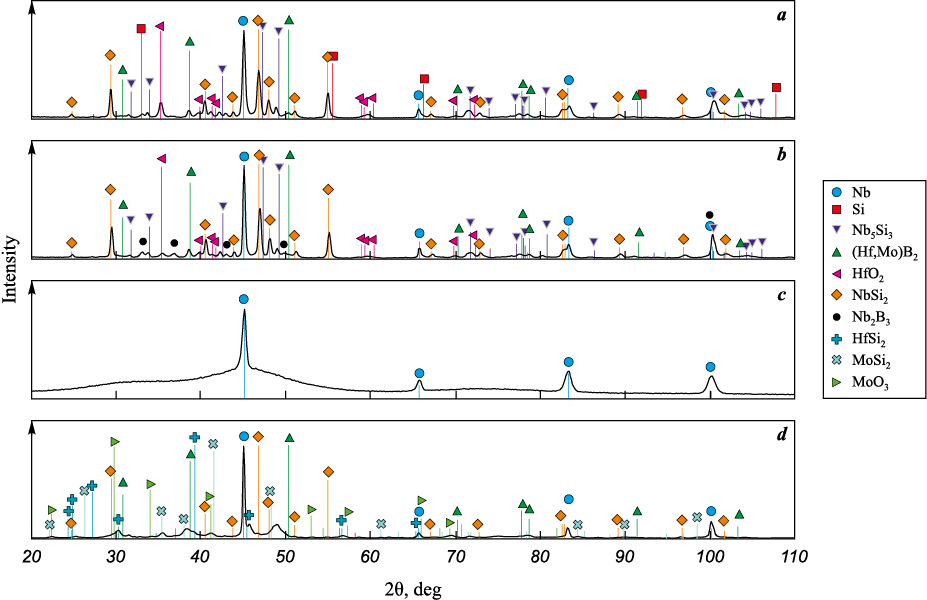
X-ray diffraction patterns of the coatings are shown in Fig. 2. The formation of NbSi2 and Nb5Si3 phases in the ESD layer – as a result of interfacial diffusion-reactions between the electrode material and the niobium substrate – indicates strong adhesion of the coating to the substrate (Fig. 2, a). The coating also contains (Hf,Mo)B2 , free Si, and HfO2 phases, consistent with the electrode composition. In the microstructure, HfO2 appears as bright inclusions (Figs. 1, a, e). After vacuum annealing, all major phases remain present at approximately the same concentrations (Fig. 2, b, Table 1). The Si phase disappears due to its reaction with the substrate, forming NbSi2 . In addition, a Nb2B3 boride phase forms in an amount of 5 wt. %.
Fig. 2. X-ray diffraction patterns of ESD (a, b) and HiPIMS (c, d) coatings
Table 1. Phase composition of ESD coatings before and after annealing
| ||||||||||||||||||||||||||||||||||||||||||||||||||||||||||||||||||||||||||
The HiPIMS coating is X-ray amorphous: the diffractogram shows only substrate reflections and broad amorphous halos (Fig. 2, c). However, after vacuum annealing, crystalline phases such as HfSi2 , MoSi2 , and (Hf,Mo)B2 are identified (Fig. 2, d). The formation of NbSi2 is attributed to the diffusion of niobium from the substrate, while the presence of MoO3 results from residual oxygen impurities in the target material. The phase analysis results are summarized in Table 2, excluding the contribution of the substrate (Nb), as the coating thickness is less than the X-ray penetration depth.
Table 2. Phase composition of HiPIMS coating after annealing
| ||||||||||||||||||||||||||||||||||||||||||
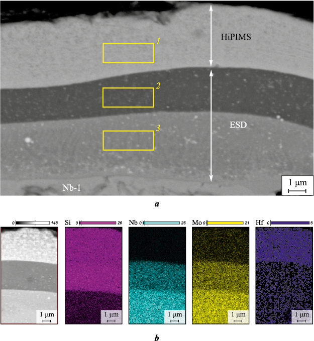
The microstructure of the ESD + HiPIMS coating after vacuum annealing is shown in Fig. 3, a. Within the electrospark-deposited layer, an outer region with a sharply defined boundary forms, corresponding to the NbSi2 phase (region 2 in Fig. 3, a, at. %: 2.9 O; 64.2 Si; 28.8 Nb; 2.1 Mo; 2.0 Hf). Bright HfO2 inclusions are observed both in the outer dark layer and in the inner layer adjacent to the substrate. According to EDS data, the inner region contains a lower silicon concentration of 28.1 at. % (region 3, at. %: 7.4 O; 28.1 Si; 48.3 Nb; 4.2 Mo; 12.0 Hf). These results indicate that heat treatment promotes silicon homogenization within the ESD layer and reduces microscale compositional inhomogeneities originating from individual mass transfer events. The magnetron-sputtered layer, which is compositionally and structurally uniform, retains its original composition after crystallization (region 1, at. %: 11.5 O; 52.8 Si; 0.5 Nb; 10.9 Mo; 24.1 Hf) and does not contribute to NbSi2 formation. The elemental distribution map confirms an increased silicon concentration in the outer ESD layer and a higher niobium content in the inner region (Fig. 3, b).
Fig. 3. Microstructure of the ESD + HiPIMS coating (а) and elemental distribution map |
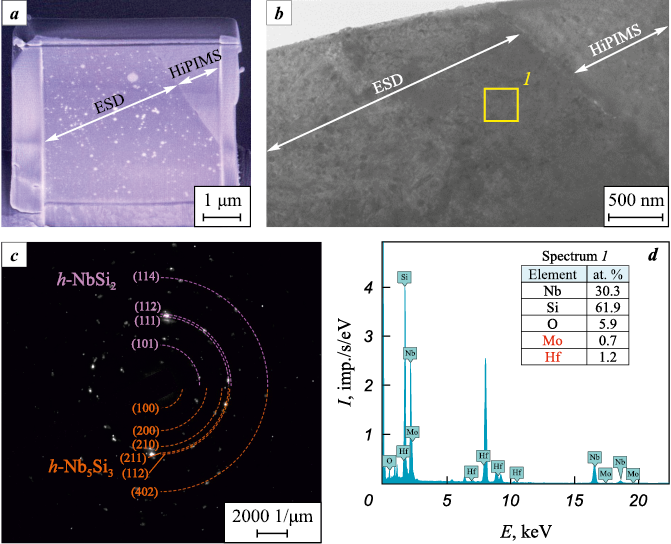
The initial lamella containing both ESD and HiPIMS layers, used for in situ investigation of structural and phase transformations during heating in the TEM column, is shown in Fig. 4, a. After cooling from 900 °C, a new layer appears at the interface with the HiPIMS coating (Fig. 4, b). According to EDS data, its composition corresponds to the NbSi2 phase (Fig. 4, c). Electron diffraction analysis confirms this identification: diffraction rings with interplanar spacings d/n = 0.356, 0.218, 0.210, and 0.136 nm correspond to the (101), (111), (112), and (114) planes of the h-NbSi2 phase. Additional rings with d/n = 0.638, 0.319, 0.240, 0.218, 0.210, and 0.140 nm, corresponding to the (100), (200), (210), (211), (112), and (402) planes, are assigned to the Nb5Si3 phase (Fig. 4, d).
Fig. 4. Microstructure of the lamella before (a) and after heating and cooling from 900 °C (b); |
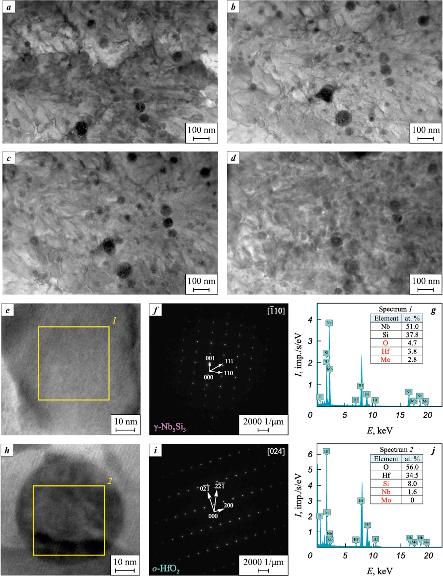
No significant structural changes were observed in the inner region of the ESD coating during heating (Figs. 5, a–c). However, after cooling the sample from 900 °C to room temperature, contrast variations appeared in certain areas. These may be attributed either to diffusion-driven elemental redistribution – accompanied by the dissolution of some structural and phase components – or to stress relaxation (Fig. 5, d).
Fig. 5. Inner layer microstructures of ESD-coating before annealing (а), during in situ heating to 400 °C (b), 800 °C (c), and after cooling from 900 °C (d); silicide phase grain (e), its electron diffraction pattern (f) |
As a result of non-equilibrium crystallization during ESD, γ-Nb5Si3 phase grains are observed in the coating, formed in the direction from the substrate toward the surface and resembling dendrites in their morphology. Dendritic growth of the metastable Nb5Si3 phase due to non-equilibrium crystallization in Nb–Si alloys has been reported in [29; 30]. A HRTEM image of a silicide grain oriented along the [\(\bar 1\)10] direction, the corresponding electron diffraction pattern, and EDS data are shown in Figs. 5, e–g. The presence of HfO2 grains, 50–100 nm in size, was also confirmed in the coating. A HRTEM image of an oxide particle oriented along the [02\(\bar 4\)] direction, together with the corresponding diffraction pattern and EDS results, is presented in Figs. 5, h–j.
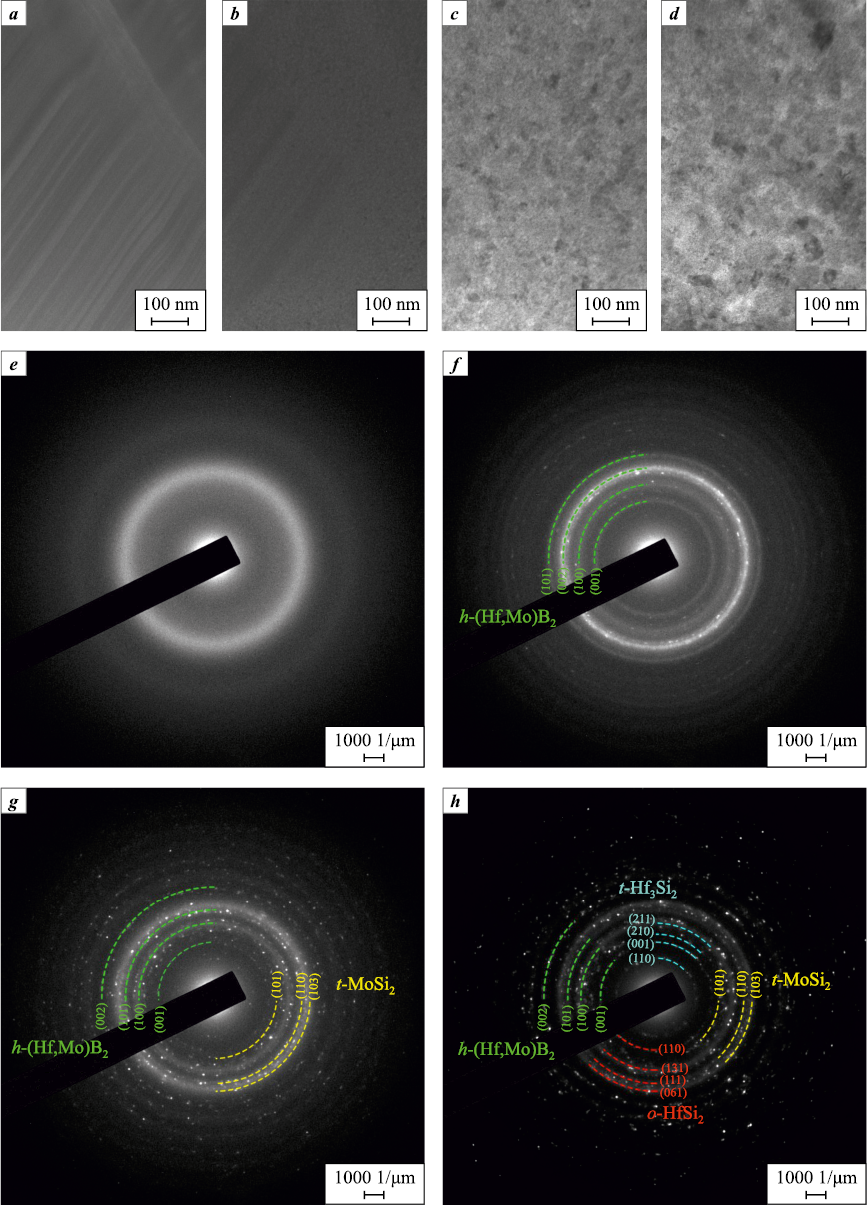
The HiPIMS coating remains stable up to 600 °C and retains a layered structure (Fig. 6, a). The corresponding electron diffraction pattern displays a broad diffuse ring, indicating that the coating is in an amorphous state. Crystallization begins at 700 °C, as evidenced by the appearance of diffraction rings with interplanar spacings of d/n = 0.355, 0.261, 0.213, and 0.178 nm, corresponding to the (001), (100), (101), and (002) planes of the (Hf,Mo)B2 phase (Figs. 6, b, f). As the temperature increases to 800 °C, additional reflections emerge at d/n = 0.291, 0.225, and 0.213 nm, attributed to the (101), (110), and (103) planes of the MoSi2 phase (Figs. 6, c, g).
Fig. 6. Microstructures (a–d) and electron diffraction patterns (e–h) of the HiPIMS coating |
Further heating to 900 °C leads to the formation of hafnium silicides. Hf3Si2 , reflections corresponding to the (110), (001), (210), and (211) planes with d/n = 0.493, 0.357, 0.309, and 0.262 nm indicate the presence of Hf3Si2 , while reflections at 0.355, 0.262, 0.226, and 0.206 nm from the (110), (111), (131), and (061) planes correspond to HfSi3 (Figs. 6, d, h). After cooling, the coating structure remained unchanged. Four crystalline phases were observed: Hf3Si2 , HfSi2 , MoSi2 , and (Hf,Mo)B2 .
Table 3 presents the hardness (H) and elastic modulus (E) values for the coatings and the substrate. The hardness of the as-deposited ESD coating is uniform across the thickness and amounts to 18.3 GPa. After annealing, the inner layer retains a hardness of H = 19.4 GPa, indicating the absence of structural transformations in the Nb5Si3-based layer. A slight decrease in the elastic modulus may be attributed to an increased Nb content due to diffusion from the substrate into the NbSi2-based layer. The hardness value of 23.3 GPa in the outer layer is attributed to the inherently higher hardness of the NbSi2 phase compared to Nb5Si3 , the absence of free niobium in this region, and alloying with niobium boride additions (Hf,Mo)B2 and Nb2B3 . For the HiPIMS coating, the hardness is H = 12.5 GPa, which corresponds to reported values for magnetron-deposited Hf–Si–Mo–B coatings [31]. After vacuum annealing and stress relaxation, the hardness decreases to 9.3 GPa. The increase in substrate hardness from 1.8 to 2.5 GPa following annealing is attributed to silicon diffusion into the interfacial region.
Table 3. Mechanical properties of coatings and Nb-1 substrate
| ||||||||||||||||||||||||||||||||||||||||||
Conclusions
1. A 15 μm-thick two-layer coating was fabricated on a Nb-1 substrate by sequential application of electro-spark deposition (ESD) and high-power impulse magnetron sputtering (HiPIMS) using HfSi2–HfB2–MoSi2 SHS-ceramic electrodes/targets. The ESD layer, ~10÷12 μm thick, consists of ~65 wt. % phases formed as a result of interfacial reactions between the electrode and the substrate, primarily NbSi2 and Nb5Si3 (H = 18.3 GPa, E = 285 GPa). A compositional gradient was observed across the ESD coating, with the Nb content increasing from 18 to 85 at. % and the Si concentration decreasing from 54 to 8 at. % from the surface toward the substrate. The HiPIMS coating has a homogeneous amorphous structure, ~5 μm thick, with H = 12.5 GPa and E = 216 GPa.
2. During heating, an interlayer ~2 μm thick based on NbSi2 forms at the interface between the ESD and HiPIMS layers (H = 23.3 GPa, E = 292 GPa). The inner ESD layer consists of dendritic grains of the metastable γ-Nb5Si3 phase solidified perpendicular to the substrate surface (H = 19.4 GPa, E = 256 GPa). Crystallization of the HiPIMS layer begins at 700 °C with the formation of (Hf,Mo)B2 . Upon further heating to 800 °C, MoSi2 appears, and at 900 °C, HfSi2 and Hf3Si2 phases are detected. After vacuum annealing, mechanical properties decrease slightly (H = 9.4 GPa, E = 207 GPa), which may be attributed to stress relaxation. Since the silicon content remains unchanged, the HiPIMS layer does not contribute to the formation of the NbSi2-based interlayer. Thus, heat treatment results in the formation of a multilayer coating with enhanced mechanical properties.
References
1. Kashin D.S., Stekhov P.A. Development of heat-resistant coatings for parts made of heat-resistant alloys based on niobium. Trudy VIAM. 2017;49(1):1–10. (In Russ.). https://doi.org/10.18577/2307-6046-2015-0-6-1-1
2. Babak V.P., Lyashenko B.A., Shchepetov V.V., Kharchenko S.D. Heat protective coatings on niobium alloys. Mechanics and Advanced Technologies. 2020;90(3):88–98. https://doi.org/10.20535/2521-1943.2020.0.219550
3. Fu T., Chen L., Zhang Y., Shen F., Zhu J. Microstructure and oxidation resistant of Si–NbSi2 coating on Nb substrate at 800 °C and 1000 °C. Ceramics International. 2023;49(13):21222–21233. https://doi.org/10.1016/j.ceramint.2023.03.252
4. Choi Y.-J., Yoon J.-K., Kim G.-H., Yoon W.-Y., Doh J.-M., Hong K.-T. High temperature isothermal oxidation behavior of NbSi2 coating at 1000–1450 °C. Corrosion Science. 2017;129:102–114. https://doi.org/10.1016/j.corsci.2017.10.002
5. Yoon J.-K., Kim G.-H. Accelerated oxidation behavior of NbSi2 coating grown on Nb substrate at 600–900 °C. Corrosion Science. 2018;141:97–108. https://doi.org/10.1016/j.corsci.2018.07.001
6. Sun L., Fu Q.-G., Fang X.-Q., Sun J. A MoSi2-based composite coating by supersonic atmospheric plasma spraying to protect Nb alloy against oxidation at 1500 °C. Surface and Coatings Technology. 2018;352:182–190. https://doi.org/10.1016/j.surfcoat.2018.07.091
7. Yan J., Liu L., Mao Z., Xu H., Wang Y. Effect of spraying powders size on the microstructure, bonding strength, and microhardness of MoSi2 coating prepared by air plasma spraying. Journal of Thermal Spray Technology. 2014;23: 934–939. https://www.doi.org/10.1007/s11666-014-0120-3
8. Yan J.-H., Wang Y., Liu L.-F., Wang Y. Oxidation and interdiffusion behavior of niobium substrate coated MoSi2 coating prepared by spark plasma sintering. Applied Surface Science. 2014;320:791–797. https://www.doi.org/10.1016/j.apsusc.2014.09.018
9. Xiao L., Zhou X., Wang Y., Pu R., Zhao G., Shen Z., Huang Y., Liu S., Cai Z., Zhao X. Formation and oxidation behavior of Ce-modified MoSi2–NbSi2 coating on niobium alloy. Corrosion Science. 2020;173:108751. https://doi.org/10.1016/j.corsci.2020.108751
10. Bukhanovskii V.V., Borisenko V.A., Kharchenko V.K., Mamuzic I. Нigh-temperature strength of niobium alloy 5VMTs with a silicide-ceramic coating. Part 1. Short-term strength characteristics. Strength of Materials. 2004;36(2):159–202. https://doi.org/10.1023/B:STOM.0000028311.58809.f9
11. Fernandes P.B., Coelho G.C., Ferreira F., Nunes C.A., Sundman B. Thermodynamic modeling of the Nb–Si system. Intermetallics. 2002;10(10):993–999. https://doi.org/10.1016/S0966-9795(02)00125-5
12. Shen F., Fu T., Zhang Y., Gao Q., Chen L. Synthesis of Si–NbSi2 coatings on Nb substrate by hot dip silicon-plating method under the various deposition temperatures. Applied Physics A. 2022;128:984. https://doi.org/10.1007/s00339-022-06129-0
13. Qiao Y., Chen T., Guo X. Diffusion barrier effect of Al2O3 layer at the interface between Mo–Si–B coating and Nb–Si based alloy. Corrosion Communications. 2021;4:45–56. https://doi.org/10.1016/j.corcom.2021.10.003
14. Yue G., Guo X., Qiao Y. Study on the diffusion barrier effect of WSi2 layer at the MoSi2/Nb–Ti–Si based alloy interface. Corrosion Science. 2020;163:108299. https://doi.org/10.1016/j.corsci.2019.108299
15. Kurokawa K., Ochiai G., Takahashi H., Ohta S., Takahashi H. Effects of sputter-deposited materials (W, Ti and SiC) on interfacial reaction between MoSi2 and Nb. Vacuum. 2000;59(1):284–291. https://doi.org/10.1016/S0042-207X(00)00281-5
16. Zhang Y., Fu T., Yu L., Cui K., Wang J., Shen F., Zhang X., Zhou K. Anti-corrosion coatings for protecting Nb-based alloys exposed to oxidation environments: A review. Metals and Materials International. 2023;29(1):1–17. https://doi.org/10.1007/s12540-022-01222-8
17. Zhang X., Fu T., Cui K., Zhang Y., Shen F., Wang J., Yu L., Mao H. The protection, challenge, and prospect of anti-oxidation coating on the surface of niobium alloy. Coatings. 2021;11(7):742. https://doi.org/10.3390/coatings11070742
18. Zhang K., Lei S., Yang R., Zhang Y., Chen S., Zhang X., Li W. Formation and oxidation behavior of SiO2/NbSi2 multilayer coating fabricated by one-step method. Surface and Coatings Technology. 2023;452:129117. https://doi.org/10.1016/j.surfcoat.2022.129117
19. Su L., Lu-Steffes O., Zhang H., Perepezko J.H. An ultra-high temperature Mo–Si–B based coating for oxidationprotection of NbSS/Nb5Si3 composites. Applied Surface Science. 2015;337:38–44. http://doi.org/10.1016/j.apsusc.2015.02.061
20. Burk S., Gorr B., Krüger M., Heilmaier M., Christ H.-J. Oxidation behavior of Mo–Si–B–(X) alloys: Macro- and microalloying (X = Cr, Zr, La2O3). JOM: The Journal of the Minerals, Metals and Materials Society. 2011; 63(12): 32–36. https://doi.org/10.1007/s11837-011-0203-2
21. Zhang P., Li Y., Chen Z., Shen C., Feng P. Preparation and moderate temperature oxidation behavior of Ti- and Al-doped NbSi2–Si3N4 composite coatings on Nb alloy. Surface and Coatings Technology. 2019;379:125005. https://doi.org/10.1016/j.surfcoat.2019.125005
22. Xiao L., Zhou X., Wang Y., Pu R., Zhao G., Shen Z., Huang Y., Liu S., Cai Z., Zhao X. Formation and oxidation behavior of Ce-modified MoSi2–NbSi2 coating on niobium alloy. Corrosion Science. 2020;173:108751. https://doi.org/10.1016/j.corsci.2020.108751
23. Zamulaeva E.I., Zinovieva M.V., Kiryukhantsev-Korneev Ph.V., Petrzhik M.I., Kaplanskii Yu.Yu., Klechkovskaya V.V., Sviridova T.A., Shvyndina N.V., Levashov E.A. Protective coatings deposited onto LPBF-manufactured nickel superalloy by pulsed electrospark deposition using MoSi2–MoB–HfB2 and MoSi2–MoB–ZrB2 electrodes. Surface and Coatings Technology. 2021;427:127806. https://doi.org/10.1016/j.surfcoat.2021.127806
24. Kiryukhantsev-Korneev P.V., Sytchenko A.D., Gorshkov V.A., Loginov P.A., Sheveyko A.N., Nozhkina A.V., Levashov E.A. Complex study of protective Cr3C2–NiAl coatings deposited by vacuum electro-spark alloying, pulsed cathodic arc evaporation, magnetron sputtering, and hybrid technology. Ceramics International. 2022;48(8):10921–10931. https://doi.org/10.1016/j.ceramint.2021.12.311
25. Kiryukhantsev-Korneev Ph.V., Kudryashov A.E., Sheveyko A.N., Orekhov A.S., Levashov E.A. Improving the oxidation resistance of Inconel 718 high-temperature nickel alloy using combined surface engineering technology. Letters on Materials. 2020;10(4):371–376. (In Russ.). https://doi.org/10.22226/2410-3535-2020-4-371-376
26. Pogozhev Yu.S., Lemesheva M.V., Potanin A.Yu., Rupasov S.I., Vershinnikov V.I., Levashov E.A. Heterophase ceramics in the Hf–Si–Mo–B system fabricated by the combination of SHS and hot pressing methods. Russian Journal of Non-Ferrous Metals. 2019;(4):380–389. https://doi.org/10.3103/S1067821219040102
27. Zamulaeva E.I., Kudryashov A.E., Kiryukhantsev-Korneev Ph.V., Bashkirov E.A., Mukanov S.K., PogozhevYu.S., Levashov E.A. Protective heterophase coatings produced by electrospark deposition and high-power impulse magnetron sputtering. Surface Engineering and Applied Electrochemistry. 2024;60(4):607–617. https://doi.org/10.3103/S1068375524700182
28. Petrzhik M.I., Levashov E.A. Modern methods for investigating functional surfaces of advanced materials by mechanical contact testing. Crystallography Reports. 2007;52(6):966–974. https://doi.org/10.1134/S1063774507060065
29. Guo Y., Jia L., Lu W., Zhang H. Morphological heredity of intermetallic Nb5Si3 dendrites in hypereutectic Nb–Si based alloys via non-equilibrium solidification. Chinese Journal of Mechanical Engineering. 2022;35:84. https://doi.org/10.1186/s10033-022-00764-7
30. McCaughey C., Tsakiropoulos P. Type of primary Nb5Si3 and precipitation of Nbss in Nb5Si3 in a Nb–8.3Ti–21.1Si–5.4Mo–4W–0.7Hf (at. %) near eutectic Nb-silicide-based alloy. Materials. 2018;11(6):967. https://doi.org/10.3390/ma11060967
31. Kiryukhantsev-Korneev Ph.V., Sytchenko A.D., Potanin A.Yu., Vorotilo S.A., Levashov E.A. Mechanical properties and oxidation resistance of Mo–Si–B and Mo–Hf–Si–B coatings obtained by magnetron sputtering in DC and pulsed DC modes. Surface and Coatings Technology. 2020;403:126373. https://doi.org/10.1016/j.surfcoat.2020.126373
About the Authors
E. I. ZamulaevaRussian Federation
Evgenia I. Zamulaeva – Cand. Sci. (Eng.), Research Scientist, Laboratory “In situ diagnostics of structural transformations” of Scientific-Educational Center of Self-Propagating High-Temperature Synthesis (SHS-Center) of MISIS–ISMAN
1 Bld, 4 Leninskiy Prosp., Moscow 119049, Russia
P. A. Loginov
Russian Federation
Pavel A. Loginov – Cand. Sci. (Eng.), Assistant Prof., Senior Researcher, Laboratory “In situ diagnostics of structural transformations” of SHS-Center of MISIS–ISMAN
1 Bld, 4 Leninskiy Prosp., Moscow 119049, Russia
Ph. V. Kiryukhantsev-Korneev
Russian Federation
Philipp V. Kiryukhantsev-Korneev – Dr. Sci. (Eng.), Professor of the Department of powder metallurgy and functional coatings (PM&FC) of NUST MISIS, Head of the Laboratory «In situ diagnostics of structural transformations” of SHS-Center of MISIS–ISMAN
1 Bld, 4 Leninskiy Prosp., Moscow 119049, Russia
N. V. Shvindina
Russian Federation
Nataliya V. Shvindina – Scientific Project Engineer, SHS-Center of MISIS–ISMAN
1 Bld, 4 Leninskiy Prosp., Moscow 119049, Russia
M. I. Petrzhik
Russian Federation
Mikhail I. Petrzhik – Dr. Sci. (Eng.), Professor of the Department of PM&FC of NUST MISIS, Leading Researcher of SHS-Center of MISIS–ISMAN
1 Bld, 4 Leninskiy Prosp., Moscow 119049, Russia
E. A. Levashov
Russian Federation
Evgeny A. Levashov – Dr. Sci. (Eng.), Prof., Corresponding Member of the Russian Academy of Sciences, Head of SHS-Center of MISIS–ISMAN, Head of the Department of PM&FC of NUST MISIS
1 Bld, 4 Leninskiy Prosp., Moscow 119049, Russia
Review
For citations:
Zamulaeva E.I., Loginov P.A., Kiryukhantsev-Korneev P.V., Shvindina N.V., Petrzhik M.I., Levashov E.A. Structure and properties of two-layer coatings in the HfSi2–HfB2–MoSi2 system produced by electrospark deposition and magnetron sputtering. Powder Metallurgy аnd Functional Coatings (Izvestiya Vuzov. Poroshkovaya Metallurgiya i Funktsional'nye Pokrytiya). 2025;19(3):48-59. https://doi.org/10.17073/1997-308X-2025-3-48-59


